Table of contents
Install
(2024-10-02)
- It has versions for Linux. Downloads
Include Libraries
References:
(2024-10-17)
- Adding Libraries in Kicad - YouTube - Electronics-PCB-Hardware Design
- Searched by
How to include 3rd party libraries into KiCADin DDG
- Searched by
Notes:
-
Click: ‘Preferences’ -> ‘Manage Symbol Libraries’ -> Click the folder icon -> Select path where the component library is:
C:\Users\ZichenWang\Documents\KiCad\8.0\3rdparty\LIB_STM8AF5288TCX\STM8AF5288TCX\KiCad
Include Footprints
References:
- How to add a .pretty directory (footprint library) - KiCad.info Forums
- Searched by
KiCad include footprintsin DDG.
- Searched by
Notes:
- Footprint editor. Docs
Draw Schematic
Search Symbols
References:
(2024-10-16)
-
Demo Project: From shematics to PCB routing and to manufacturer Learn KiCad 8 in 45 minutes - From idea to upload in one video - YouTube - AnotherMaker
- Searched by
kicad 8 tutorialin DDG
- Searched by
-
What component to use for “pin headers”? - KiCad.info Forums
- Searched by
KiCad symbol 4 Headerin DDG
- Searched by
Notes:
- Search keyword: “CONN” for Connecters r1
TestPoint
Start: Don’t know what this symbol is:


Reference:
(2024-10-18)
- Create bottom test points on the circuit board as … - KiCad.info Forums
- Qingjun said: Those are 测试点
- Search:
KiCad add testing pointin DDG
Notes:
-
TestPoint symbol and footprint Forum
-
Footprint for TestPoint Footprint Library - TestPoint - GitHub Pages (Searched by s1)
Hierarchical Sheets
Reference:
(2024-10-18)
-
KiCad 5 #16 Multisheet Schematics - YouTube - John’s Basement
- I wanted to draw an exactly same copy of the sample schematic, which spilt the entire circuit into multiple cells.
- Search:
how to split the schematic diagram into cells in KiCADin Google
-
Multiple schematic pages in one project - KiCad.info Forums
- Searched by
Kicad add additional pagein DDG
- Searched by
Notes:
-
Feels it’s like a “hyperlink” to enable jumping to another sheet. r1
Tricks:
-
Connecting two components with a wire, allowing streching when moving around.
-
Numbering components across sheets by x100
-
Delete debug markers: “Electrical Rules Checker” -> “Delete All Markers” 12:19
-
-
KiCad doesn’t support multiple sheets, in favor of hierarchical sheets. r2
Labels
Reference:
(2024-10-18)
-
开源EDA软件kicad6.0讲解之十二-原理图连接方式,网络标签,总线放置,标签语法详解 -bilibili- 含羞草的367朵花
- Search
kicad 绘制原理图in bilibili - Open: 开源EDA软件kicad6.0讲解之十三-多原理图设计,原理图分页,全局标签,分模块设计 - 含羞草的367朵花
- Went to the previous video laying out basics.
- Search
-
Connecting nets without wires on schematic - Page 1 - EEVblog
- Searched by
KiCad connection name and Net namein DDG
- Searched by
-
- Searched by
KICad connection namein DDG
- Searched by
-
Docs - Schematic Creation and Editing
- Searched by
kicad net namein DDG
- Searched by
Notes:
-
Same text means a common connection. r1
-
Pressing L to add a Local label across the current sheet.
-
Tricks:
- Pressing
Inskey to adding repeating objects. - Pressing
~to highlight the network.
- Pressing
-
-
Create a “Net Name” for a connection by the tool: “Add Label” r2:
(2024-10-19)
-
Is a “GND” symbol not connected with a “GND” net name?
GND Symbol GND Label 


Marks on Sheet
Reference:
(2024-10-18)
-
#4 How To Prettify Your Schematic with Kicad 7.0 | #PCBCupid - YouTube
- Directed by the video: #8 How To Use Constraints And Net Class Directive tool in KiCad 7.0 | #PCBCupid - YouTube, which shows a schematic with cells layout. Then, I went to check their other videos in this playlist.
- This video is searched by “Kicad add net class directive” in DDG, when I wonder what’s the button ‘Add Net Class Directive’ below ‘Add Label’, which I was about to try.
Notes:
-
Each functional unit can be fenced by “Adding a rectangle” forming a “cell”.

Simulation
(2024-10-16)
-
Start: I first saw the word “Simulation” is in the title: “Simulation Workflow Best-Practise for a Complete Project” (Searched by
STM8AF5288 in kicad projectin DDG) -
Story: Although the chip STM8AF6223, which is available in KiCad, doesn’t have USART, I can implement the LIN circuit first.
Then, I started thinking if there is a possible way to verfiy my circuit… How can I see the wave shapes? Can I use a virtual oscilloscope to probe the output? I remember I did some simulation experiments using a software called “Proteus” in my undergraduate course.
Can KiCad do simulation? Right, it possibly does, as I just saw the searched result.
Searches
(2024-10-16)
-
Search:
Kicad 8 simulationin DDG-
Introductory videos on simulation with ngspice in KiCad 8 - Forum
-
Two resistors series connection. Power supply used the
VDCin the Simulation_SPICE library.
-
Oscilloscope visualization the input and output voltage across an operational amplifier. ngspice in KiCad 8: inverting amplifier with generic opamp
-
-
A descriptive introduction post: KiCad 8: Working with Circuit Simulations! - element14 Community
-
NE555 LED
Reference:
(2024/10/17)
-
- Searched by
KiCad 8 simulation for LEDin DDG
- Searched by
-
SPICE libraries download links:
Missing Model Simu Files
(2024-10-17)
-
Search:
Kicad spice simulation filein DDG -
Kaushik:
-
Make a package by yourself
-
Search in websites:
-
-
Attach simulation model

I2C Simu
(2024-10-17)
-
Search
I2C simulation in KiCad 8in DDG
Make Symbol
Reference:
(2024-10-18)
-
Symbol for a passive component (Inductor): KiCad初学者 - 第2集 创建元件符号(A) - Michael_AU
- Recommended by Qingjun.
-
Symbol for an IC (Controller for Boost): KiCad初学者 - 第3集 创建元件符号(B)- Michael_AU
(2024-10-22)
Notes:
(2024-10-19)
-
Steps:
-
Symbol Editor
-
File -> New Library -> Add To Library Table -> Global (For being searchable in other projects)
-
Symbol file path:
C:\Users\ZichenWang\Documents\ECU_Practice-Zichen-2024-10-16\3rd_Party_Libs\Conn_Zichen.kicad_sym -
New Symbol -> Fill out properties:

-
Symbol name: TC2030-MCP-NL
-
Default reference designator: J
-
The rest attributes are left as default
-
Add Pin (P) -> Set properties:
-
Pin name:
-
Pin number:
-
Electrical type:
- Inductor is a passive component; While pins of IC require Electrical Types.
- Power and Analog GND are supposed to be “Power Input” type.
-
Orientation
-
-
Draw graphical shapes
-
Edit Symbol Properties:
-
Reference: J
-
Value: TC2030-MCP-NL
-
Footprint:
-
MPN (Manufacturer part number? for exporting BOM)
-
Manufacturer: Microchip Technology
-
Description: PLUG-OF-NAILS 6-PIN W/O LEGS
-
DigiKey Part Number: TC2030-MCP-NL-ND
-
The “Pin Table” in “Symbol Editor” provides an overview for all pins. 07:46
-
-
Modify graphical shape properties by double-clicking it
- Fill with body background color
-
Make Footprints
References:
(2024-10-19)
-
Images of TC2030 are from:
Notes:
-
Steps (r1):
-
Open “Footprint Editor” 05:48
-
Set up plotting workspace 06:01
-
Specify unit (inches,mils,mm) and grid size
-
The positive direction of y is down.
-
-
File -> New Library -> Global 07:27
-
Custom library foder (.pretty) storage path:
C:\Users\ZichenWang\Documents\ECU_Practice-Zichen-2024-10-16\3rd_Party_Libs\Conn_Zichen.pretty -
The newly created lib may not be inlcuded in search path yet (KiCad 5.1.10).
-
-
File -> New Footprint 09:11
-
Read datasheet for pads sizes and layout
-
Enter footprint name for this component: TC2030-MCP-NL-FP

-
Footprint type: SMD
-
To move texts, pressing key ‘M’
-
-
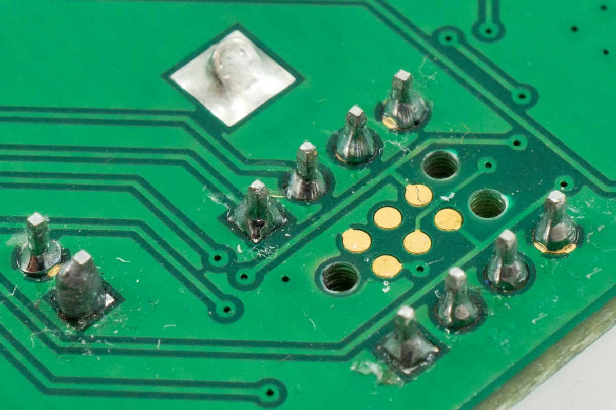
Place pads: “Add Pad” 11:42
-
The 3 outer triangle vertices seems through hole for “Alignment pins”
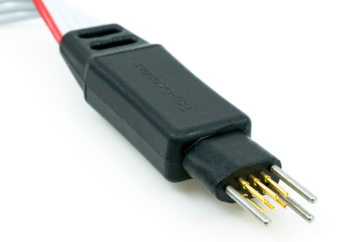
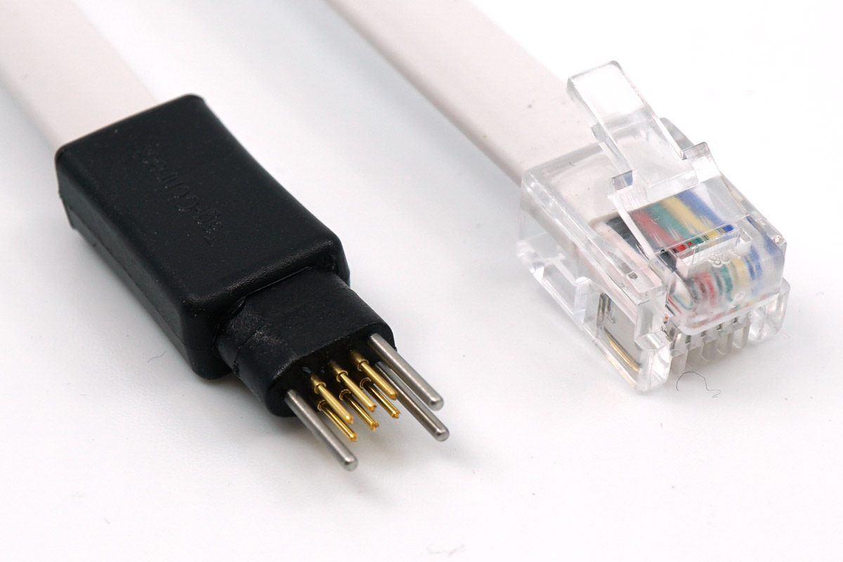
Interface Footprint Outlook Pins of TC2030 RJ12 for ICD 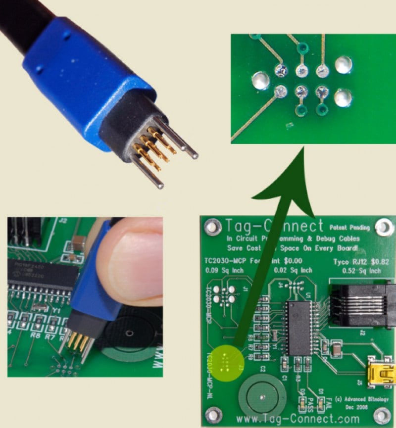
-
“Add Pads” with type:
Through-holefor the 3 “locating holes”.
-
Add 6 pads with type
SMD(Surface mounted 贴片)
-
-
Draw frames (placeholder) on the layer: F.Silkscreen (Front of Silkscren 丝印层的顶层) 14:24
-
Datasheet instruction: “No other track or signal within 0.020” of any contact pad."
I drew the illustration for “Optional Bottom Layer”

-
Adjust the texts position
-
-
Add 3D model (.step) file 16:25
-
Obtain 3D model from the seller official website and models download website
-
“Footprint Properties” -> “3D Models”

-
Look around the 3D model to check whether the pins match the pads
-
-
Link the footprint to the symbol 19:50
-
“Symbol Editor” -> “Symbol Properties” -> “Footprint”.

-
-
-
Make footprint for an IC chip with “templates” 21:58
- File -> “Create Footprint” (Create a new footprint using the Footprint Wizard)
