Table of contents
(Feature image from:
YuanBiju/serial-communication-protocols
Searched by Serial communication protocol in DDG image)
I2C Bus
Comm Protocol
I2C: Inter-Integrated Circuit
-
Master and Slave
-
Allow multiple master, however, only 1 master at a time
-
The first device making a falling edge to the bus while the SCL is in high stage (a start signal) will occupy the bus exclusively, until this device making a rising edge when the SCL is high.
-
-
Two wires: SCL (serial clock) and SDA (serial data)
-
The SCL signal determines when to sample the SDA.
- Therefore, the slave can stall the master by holding the SCL line low longer. (r4-GfG)
-
-
Default (recessive, idle) state is a high voltage (
1) because of the pull-up resistors.
::: aside
- References: {{{
-
I2C Communication Protocol - GeeksforGeeks
Searched byi2c protocol and UML sequence diagramin DDG }}} :::
-
I2C Communication Protocol - GeeksforGeeks
-
Serial transmission: the signal on the SDA is transferred byte-by-byte
-
There is a Receiver response after every byte (8 bits).
-
Following the Start condition, the first byte is a 7-bit device address plus a Read/Write bit, followed by a ACK bit from the receiver. The second byte is an address of a memory in the device, followed by a ACK bit from the receiver. The third byte is a 1-byte data to be transferred, followed by a ACK bit from the receiver.
-
Higher bits are transmitted first
-
-
Single data wire (Half-duplex):Transmit and receive share a common wire.
-
Bidirectional, i.e., the data flow direction can flip between master and slave.
-
Master and slave cannot talk at the same time (r2-半双工).
-
Communication means just 2 operations: Write or Read. The master sends out an instruction of writing data to a device, or requesting data from a device.
::: aside
::: -
Bus status
-
4 Phases
-
Transferring starts when the bus appears that: the SDA falls down when the SCL is a high voltage.
-
Transferring stops when the bus shows that: the SDA raises up when the SCL is a high voltage.
-
Data transmission: SDA makes change when SDL is low, and keeps consistant during SDL is high (r5-CSDN).

-
Receiver Response: Every 8 bits (1 byte), the SDA should be a low voltage, representing
ACK, whereas a high voltage (recessive) indicatesNACK: the byte just sent was not received successfully.
::: aside
::: -
Frame Structure
-
Start condition: SDA drops turnning to dominant level (0), triggering the SCL to oscillate.
-
Device Address: 7 bits (allowing max 128 devices mounted on the I2C bus)
-
The voltage on SDA needs to keep consistant during the entire high phase of the SCL.
-
The frame will be broadcasted and captured by all slaves, and only the matched device will response.
-
-
Read / Write: 1 bit,
0for Writing and1for Reading.-
When the master is sending data to the slave, SDA is
0(dominant) at this bit; -
Whereas
1indicates the master is receiving data from the slave.
-
-
Transferring one byte needs 9 bits. In contrast, the data field of a LIN frame is 10 bits.
-
I noticed that the voltage change representing a 1-byte data only occurs when the SCL is low.
Is that the reason for designing the start and stop conditions as the voltage changes occur when SCL is high?
In other words, the occurence of the ‘voltage change’ on SDA differentiate the two fields: Start/Stop bits and data/ACK field.
-
There is NO repeated Start/Stop bits between bytes transferring, i.e., the next byte will be directly transferred after the
ACKbit, as shown in the following wave shape (r3-EEWorld):
::: aside
:::References
{{{ 1. [树莓派开发I2C介绍 - 石然老师](https://www.bilibili.com/video/BV11F411g7cN/)
Searched by `树莓派 i2c 通信` in [Bilibili](https://search.bilibili.com/all?vt=48473987&keyword=%E6%A0%91%E8%8E%93%E6%B4%BE%20i2c%20%E9%80%9A%E4%BF%A1&from_source=webtop_search&spm_id_from=333.1007&search_source=5) 3. [示波器和I2C时序波形图的关系分析-电子工程世界](https://news.eeworld.com.cn/Test_and_measurement/ic486741.html)
Searched by `I2C 示波器 波形 电子发烧友` in [DDG Images](https://duckduckgo.com/?q=I2C+%E7%A4%BA%E6%B3%A2%E5%99%A8+%E6%B3%A2%E5%BD%A2+%E7%94%B5%E5%AD%90%E5%8F%91%E7%83%A7%E5%8F%8B&iax=images&ia=images) Referenced by [r1-Bili](#I2C-r1) 6. [What determines I2C interrupt service time after address byte ACK? - SE](https://electronics.stackexchange.com/q/719068)
Found by search [image](#I2C-wav-r5) in Google }}}

Write-Data Frame
References:
- 4分钟看懂!I2C通讯协议 最简单的总线通讯! - 爱上半导体
- Searched by
I2Cin Bilibili
- Searched by
Notes:
-
Example of writing a 1-byte data into an EEPROM chip.
-
EEPROM chip: 24C02 has 256 bytes (256 × 8-bit) memory. Datasheet
-
The memory address
0x01will be written into the register of the EEPROM chip (? Not sure), and the data0x0Fwill be stored in the memory.
-
Read-Data Frame ❌
- A read data frame consists of one write operation followed by one read operation.
-
The address of memory to be read is
0x01, which will be put into a register in the EEPROM chip (? Not sure.)(2024-10-26)
- The “empty” write command may aim to locate the target memory in the EEPROM. Simu-I2C-CSDN
-
Question: If the slave is MCU, why the “Slave address” after the second Start bit is still the address of the EEPROM?
I2C on Arduino
::: aside
- References: {{{
2.
Inter-Integrated Circuit (I2C) Protocol - Arduino Docs
Searched byI2C on arduinoin DDG 3. Wire - Arduino Reference
Found in: Docs Home -> ‘Rapid Access’: Language Reference }}} :::
Notes:
-
The
<Wire.h>library implemented the underlying I2C protocol and is included in all Arduino board packages. So one only need to call its API to transfer data with I2C. (r2-Docs) -
Initializing
WireandSerialfor I2C transmission and printing data to console.-
Calling the derived library for a specific device, e.g.,
<Adafruit_MPU6050.h>to communicate is more convinent than calling the lower-leverWire.hlibrary. -
“Adafruit” is the organization that developed the ‘STEMMA QT’ connector.
-
The device identifier and the number of bytes to be read needs to be specified in the instruction forming function:
requestFrom(device_id, n_bytes). -
To read one byte from the bus:
Wire.read(). To check how many bytes left on the bus:Wire.available()(r3-Docs). -
To write bytes onto the bus:
Wire.write()
\begin{algorithm} \caption{Master Reads 6 Bytes} \begin{algorithmic} \REQUIRE{Wire.h} \FUNCTION{setup}{} \STATE{Wire.begin()} \STATE{Serial.begin(9600)} \COMMENT{For serial monitor} \ENDFUNCTION \FUNCTION{loop}{} \STATE{Wire.requestFrom(8, 6)} \COMMENT{request from device 8 for 6 bytes} \WHILE{Wire.available()} \COMMENT{read byte one-by-one until the countdown reaches 0} \STATE{char c = Wire.read()} \STATE{Serial.print(c)} \ENDWHILE \STATE{delay(500)} \ENDFUNCTION \end{algorithmic} \end{algorithm}-
The program running on the slave should declaim the identifier for the slave at the begining:
Wire.begin(8) -
The responser sends data hardly when it received the request instruction by executing
onRequestfunction -
The slave only response once, so the data is only
write()once in thesetup()function. -
One character is a byte.
\begin{algorithm} \caption{Device Responses 6 Bytes} \begin{algorithmic} \FUNCTION{setup}{()} \STATE{Wire.begin(8)} \ENDFUNCTION \FUNCTION{loop}{()} \STATE{delay(100)} \ENDFUNCTION \FUNCTION{onRequest}{()} \STATE{Wire.write("hello ")} \ENDFUNCTION \end{algorithmic} \end{algorithm} -
Simu I2C
-
Problems:
- Start: I wondered what does the wave of a read frame look like.
-
Supports:
-
The first bare write command without writing any data is called “伪写入” Simu-I2C-CSDN
-
I2C waveform r3-OfficialTut
- Observing I2C waveform using a logic analyzer on Wokwi r5-Docs
::: aside
**References**: {{{-
基于proteus仿真的单片机IIC(I2C)通信(超详细) - CSDN
- Searched by
Proteus 仿真 I2C 通信in DDG
- Searched by
-
- I2C总线协议,STM32单片机在proteus仿真实例代码讲解 - bilibili - sfdsl1
- Searched by
I2C 电路仿真(2024-10-17) in bilibili
- Searched by
- Interal tutorial page in the ‘Getting Started’ section of Proteus 8 Demonstration.
-
Proteus Tutorial : Proteus VSM for Arduino - YouTube - Labcenter Electronics Ltd
- Searched by
Proteus VSM Tutorialin DDG
- Searched by
-
逻辑分析仪使用指南 | Wokwi Docs
- Searched by
逻辑分析仪 用法in DDG
- Searched by
Haptic Motor Driver
-
Problems:
-
How to control a haptic motor?
-
Haptic motor driver:
DRV2605LDGSTr2-Datasheet -
I2C address of
Sparkfun Haptic Motor Driver - DRV2605L(ROB-14538):0x5Ar3-Intro

-
::: aside
:::References:
{{{ 2. [Datasheet: DRV2605L 2- to 5.2-V Haptic Driver for LRA and ERM with Effect Library and Smart-Loop Architecture (pdf)](https://www.ti.com/lit/ds/symlink/drv2605l.pdf)
Searched by `DRV2605LDGST` at [DDG](https://duckduckgo.com/?q=DRV2605LDGST&ia=web) 3. [Breakout Introduction: SparkFun Haptic Motor Driver - DRV2605L - Digi-Key](https://mm.digikey.com/Volume0/opasdata/d220001/medias/docus/778/ROB-14538_Web.pdf)
Searched by `Sparkfun Haptic Motor Driver - DRV2605L` at [DDG](https://duckduckgo.com/?q=Sparkfun+Haptic+Motor+Driver+-+DRV2605L&ia=web) 4. [Haptic Motor Driver Hook-Up Guide - SparkFun Learn](https://learn.sparkfun.com/tutorials/haptic-motor-driver-hook-up-guide/all) 5. [SparkFun Haptic Motor Driver - GitHub](https://github.com/sparkfun/Haptic_Motor_Driver) }}} -
➀ Connection Arduino and DRV2605L
-
Problems:
- How to connect an Arduino to the SparkFun Haptic Motor Driver (DRV2605L)?
::: aside
- References: {{{
-
Supports:
-
INis Multi-mode input. I2C is selectable as PWM, analog, or trigger. If not used, this pin should be connected to GND Datasheet Sec 5. -
ENcontrols the power state Datasheet Sec 8.4.1, logic high. Datasheet Sec 9.3.1 -
SDA and SCL Datasheet Sec 8.5.3
-
Connection to application processor Datasheet Sec 9.1.

::: aside
:::References
{{{ 1. [GPT5 Pro - Arduino SparkFun connection guide](https://chatgpt.com/c/68f67d1d-c4a0-8331-96db-037b33206b56) }}} -
-
Actions:
-
Pins of the driver board
Pin To GND GND VCC Nano 5V Out SDA Nano A4 I2C Data SCL Nano A5 I2C Clock IN GND EN Nano 5V Out -
Observe voltage between Out pins
The driver board preserves a default firmware already.
The default firmware for the DRV2605L is set for use with ERM type motors. Tutorial
-
➁ Registers Definition of DRV2605L
-
Problems:
- Use Arduino Nano to control an LRA motor to generate haptic motion
-
Supports:
-
Registers settings for Internal Trigger Mode r1-Learn
-
MODEbits (Addr:0x01, lowest 3 bits)Sec 8.4.2: Mode selection register –> 0 (Internal trigger mode)Table 2 -
Feedback control (Addr:
0x1A)Sec 8.6.200x00110110(0x36) –>0(ERM mode);011(4x feedback gain ratio between braking gain and driving gain);01(Medium loop gain for the feedback control);10(For ERM motor, 1.365x analog gain of the back-EMF amplifier.) -
Library Selection register (Addr:
0x03, lowest 3 bits)Sec 8.3.5.2:LIBRARY_SEL–> 2 (Library B for ERM)Table 1 -
Eight waveform sequencer register (Addr:
0x04~0x0B) storing “waveform identifier”, the index of waveform in a ROM library, will be read to play the corresponding waveform. -
GO register (Addr:
0x0C) remains high until the playback of the haptic waveform sequence is complete.
Arduino Code
{{{ ```cpp #include//SparkFun Haptic Motor Driver Library #include //I2C library SFE_HMD_DRV2605L HMD; //Create haptic motor driver object
void setup() { HMD.begin(); // Read Status register Serial.begin(9600); HMD.Mode(0); // Internal trigger input mode – Must use the GO() function to trigger playback. HMD.MotorSelect(0xB6); // ERM motor, 4x Braking, Medium loop gain, 1.365x back EMF gain HMD.Library(6); //1-5 & 7 for ERM motors, 6 for LRA motors
} void loop() { int seq = 0; //There are 8 sequence registers that can queue up to 8 waveforms for(int wave = 1; wave <=123; wave++) //There are 123 waveform effects { HMD.Waveform(seq, wave); // Write the waveform identifier
waveto the register seq HMD.go(); // Start play waveforms delay(600); //give enough time to play effect Serial.print(“Waveform Sequence: “); Serial.println(seq); Serial.print(“Effect No.: “); Serial.println(wave);if (wave%8==0) //Each Waveform register can queue 8 effects { seq=seq+1; } if (wave%64==0) // After the last register is used start over { seq=0; }} }
1}}} -
::: aside
:::References
{{{ 1. [Haptic Motor Driver Hook-Up Guide - SparkFun Learn](https://learn.sparkfun.com/tutorials/haptic-motor-driver-hook-up-guide#:~:text=example%20in%20detail.-,Internal%20Trigger%20Mode,-The%20internal%20trigger) }}} -
-
Actions:
-
Connect a motor (got from John)

-
-
Results:
-
Iterate 123 effects in the interal-ROM library Datasheet Sec 8.3.5.2:

-
I2C on Renesas
➀ SmartConfig Gen I2C For RL78-F23
-
Problems:
- Use
Smart Configuratorto generate I2C driver code
- Use
-
Supports:
-
I2C component configuration on the Sample Code of Multi-slave r1-Sample


- According to the circuit schematic, pins
p11andp12are used for I2C, corresponding to the simplified I2C function, rather than “IICA”
::: aside
:::References
{{{ 1. [RL78/G23 I2C Supporting Multiple Slave Address (Master) Rev.1.00 - Sample Code - R01AN5825XX0100](https://www.renesas.com/en/search?keywords=rl78%20i2c&type=Documents#:~:text=RL78/G23%20I2C%20Supporting%20Multiple%20Slave%20Address%20(Master)%20Rev.1.00%20%2D%20Sample%20Code) }}} -
-
Actinos:
-
If enabling the SER00 merely, the default pins are not p11 and p12.
I manually set the p11 and p12 to be used as serial.
-
APIs of IICA
-
Problems:
- Functions of starting I2C transmission from the sample code for G23 r1-Code
::: aside
:::References
{{{ 1. [RL78/G23 I2C Supporting Multiple Slave Address (Master) Rev.1.00 - Sample Code](https://www.renesas.com/en/document/scd/rl78g23-i2c-supporting-multiple-slave-address-master-sample-code?queryID=c2b867e0601d8a2a2274a2a639faa841) }}}
➀ Read Data to 7-bit Addr
-
Problems:
-
Read 256 bytes starting at address 0x00:
1status = R_IICA0_Rx(sladr, 0x00, g_Rx_buff, 256);
-
-
Supports:
-
Definition:
1
2
// src\smc_gen\Config_IICA0\Config_IICA0_user.c uint8_t R_IICA0_Rx(uint8_t sladr7, uint8_t adr, uint8_t * const rx_buf, uint16_t rx_num)-
Slave address (7 bit address):
sladr -
Read starting address:
0x00 -
Received data pointer:
g_Rx_buff -
Receive data number:
256
-
-
➁ Write Data to 7-bit Addr
-
Problems:
-
Write 16 bytes data to slave
1
2
3
4
5
for ( i = 0 ; i <16 ; ++i ) { /* transmit 16 bytes data to slave */ txbuf = (uint8_t *)&INC_DATA[i][0]; status = R_IICA0_Tx(sladr, i*16, (uint8_t *)txbuf, 16); }
-
-
Supports:
-
Definition
1uint8_t R_IICA0_Tx(uint8_t sladr7, uint8_t adr, uint8_t * const tx_buf, uint16_t tx_num);-
Slave Address:
sladr -
Writing address:
i*16 -
Data to be sent:
txbuf -
Number of bytes to be sent:
16
-
-
➂ Read/Write to 8-bit Addr
-
Problems:
-
Read data
1status = R_IICA0_Master_Receive((sladr << 1 ), &g_Rx_buff[(i*16)], 16 ); -
Write data:
1status = R_IICA0_Master_Send((sladr << 1 ), g_Tx_buff, 257 );
-
-
Supports:
-
Definition
1uint8_t R_IICA0_Master_Receive(uint8_t sladr8, uint8_t * const rx_buf, uint16_t rx_num)- Slave address 8-bit:
sladr - Data to be read:
rx_buf - Number of bytes:
rx_num
- Slave address 8-bit:
-
Difference from
R_IICA0_RxR_IICA0_Rxrequires data pointeradr(in the slave memory), whileR_IICA0_Master_Receivedoesn’t, so it should be used when theadr, i.e. (interal) address register is set r1-GPT
::: aside
:::References
{{{ 1. [GPT5 - Explain code functionality](https://chatgpt.com/c/68fa4028-666c-8329-bf86-fa8c930608db) }}} -
RL78-F23 Controls Haptic
-
Problems:
- Use RL78/F23 haptic ECU to contol the haptic motor driver board
-
Supports:
-
I2C Frame of Writing the Mode Selection Register 0x01
-
➁ I2C Multiplexer NCA9548A
-
Problems:
-
Identical parts have the same I2C address on the bus, so the MCU cannot individually control each component
Therefore, a “switch” is used to select one of the components.
::: aside
:::References
{{{ 1. [Gemini 2.5P - I2C Switch for Identical Haptic Motors](https://gemini.google.com/share/67102feee696) 2. [NCA9548APW (8-channel I2C-bus switch with reset) | Nexperia](https://www.nexperia.com/product/NCA9548APW) }}} -
-
Supports:
-
SDA for selecting channel 0
Write the control register:
- first byte:
0x11100000(0x70 + 0) - second byte:
0x01
- first byte:
-
-
Actions:
-
Write 1 byte to the address
-
Write-Read Register of NCA9548A
-
Problems:
-
Set flag variables for transmission completion
-
RL78-F23 Read DRV2605L
Remove StopCondition From Callback
-
Problems:
-
The variable that monitors a target register does not change after a single write-read sequence.
1
2
3
4
5
6
7
8
9
uint8_t watch_mod=1; void main(void) { // Write 0 to register 0x01 drv2605l_write_reg(0x01, 0x00); // Read the value in the register 0x01 drv2605l_read_reg(0x01, &watch_mod); }- The value of
watch_moddoesn’t change, maintaining its initial value.
As a result, it’s unclear whether the write or the sebsequent read is failing.
- The value of
- TL;DR Answer: The callback only set the communication completion flag.
-
-
Supports:
-
In a simplified IIC reading flow, singals comparison of issuing a
StopCondition()immediately after the write v.s. issuing a repeated Start are illustrated below. r1-Forum{{{
}}}Read without stop condition Read with stop condition R_IIC00_Master_Send(0XC0, data_buf_tx, 1); while(IIC00_flg_end == 0) { NOP(); } IIC00_flg_end = 0; // R_IIC00_StopCondition(); <----- //IIC00_flg_end is set to 1 when interrupt is generated R_IIC00_Master_Receive(0XC0, data_buf_tx2, 2); while(IIC00_flg_end == 0) { NOP(); } IIC00_flg_end = 0; R_IIC00_StopCondition();R_IIC00_Master_Send(0XC0, data_buf_tx, 1); while(IIC00_flg_end == 0) { NOP(); } IIC00_flg_end = 0; R_IIC00_StopCondition(); //IIC00_flg_end is set to 1 when interrupt is generated R_IIC00_Master_Receive(0XC0, data_buf_tx2, 2); while(IIC00_flg_end == 0) { NOP(); } IIC00_flg_end = 0; R_IIC00_StopCondition();

-
Based on the DRV2605L datasheetSec 8.5.3.5, a single-byte read uses a repeated start condition, between the address/write phase (for register pointer) and the address/read phase, there is not a stop condition in between. Instead, a start condition (belonging to the address/read phase) follows.

- The bus should do: StartCondition –> SlaveAddr+W —> RegAddr —> StartCondition –> SlaveAddr+R –> DataBuf
-
I realized a “Repeat start condition” doesn’t include a stop condition while I was explaining my code to Jackie, when I noticed there is not a dropping edge, as a stop condition appears.
-
There must not be a stop condition after the initial write phase that sets the register pointer; there must be the start condition of the read phase.
-
If a StopCondition is inserted, the device won’t treat the preceding write as the prerequisite pointer write for the following read.
-
The paragraph above the timing diagram already describes the correct bus signals, but I initially overlooked it.
-
Jackie inspired me that the
StartConditionandStopConditionare practical elements consituting the protocal implementation, during she reviewed my code.
::: aside
:::References
{{{ 1. [RL78/G13 - Not able to generate repeated start using simplified I2C(SDA00) - RL78 MCU Forum | Renesas Engineering Community](https://community.renesas.com/mcu/rl78/f/rl78-forum/28849/rl78-g13---not-able-to-generate-repeated-start-using-simplified-i2c-sda00?queryID=bf2e67bb2347628dfa3326f8038c49c2)
Searched by `rl78 simplified i2c sample code` at [Search | Renesas](https://www.renesas.com/en/search?keywords=rl78%20simplified%20i2c%20sample%20code) }}} -
-
Actions:
-
R_IIC00_StopCondition()should not be called inside the ISR callback, because the Stop condition is not always the correct bus action at the end of a write phase. some transactions require an immediate Start condition to read depending on specific devices.The stop
R_IIC00_StopCondition()should only be issued at the point where the entire IIC communication concludes. -
The callback function only set the flag that signal the current data phase is done.
 1
 2
 3
 4
 5
 6
 7
 8
 9
10
11
12
13
14
15
16
17
18
19
20
21
22
// Config_IIC00_user.c #define DRV2605L_ADDR7 0x5A static volatile uint8_t i2c_done = 0; static volatile uint8_t i2c_err = 0; static void r_Config_IIC00_callback_master_sendend(void) { // R_Config_IIC00_StopCondition(); /* STOP after write */ i2c_done = 1; } static void r_Config_IIC00_callback_master_receiveend(void) { i2c_done = 1; } static void r_Config_IIC00_callback_master_error(MD_STATUS flag) { R_Config_IIC00_StopCondition(); i2c_err = (uint8_t)flag; i2c_done = 1; }- These functions are called in the ISR
r_Config_IIC00_interrupt()
- These functions are called in the ISR
-
Write register
 1
 2
 3
 4
 5
 6
 7
 8
 9
10
11
12
13
// Write 1 register (reg, val) in a single I2C transaction MD_STATUS drv2605l_write_reg(uint8_t reg, uint8_t val) { uint8_t tx[2] = { reg, val }; i2c_done = i2c_err = 0; R_Config_IIC00_Master_Send((uint8_t)(DRV2605L_ADDR7<<1), tx, 2); while(i2c_done == 0) { /* wait */ NOP(); } R_Config_IIC00_StopCondition(); // Followed by a StopCondition after writing done return i2c_err ? MD_ERROR1 : MD_OK; } -
Read register
 1
 2
 3
 4
 5
 6
 7
 8
 9
10
11
12
13
14
15
16
17
18
19
20
// Read 1 register (does a pointer write, then a read) MD_STATUS drv2605l_read_reg(uint8_t register_addr, uint8_t *val) { i2c_done = i2c_err = 0; R_Config_IIC00_Master_Send((uint8_t)(DRV2605L_ADDR7<<1), ®, 1); while(i2c_done == 0) { /* wait */ NOP(); } // Don't append StopCondition, since another StartCondition is required. i2c_done = i2c_err = 0; R_Config_IIC00_Master_Receive((uint8_t)(DRV2605L_ADDR7<<1), val, 1); while(i2c_done == 0) { /* wait */ NOP(); } // Followed by a StopCondition after reading done R_Config_IIC00_StopCondition(); return i2c_err ? MD_ERROR1 : MD_OK; } -
Write and read the
0x01register1 2 3 4 5 6 7 8 9 10 11 12 13 14 15 16 17 18 19 20 21 22 23 24 25 26 27 28 29 30 31 32 33 34 35 36 37// main.c #include "r_smc_entry.h" #include "src/multiplexer.h" #include "src/drv2605l.h" void main(void); uint8_t watch_mod=1; void main(void) { R_Config_IIC00_Create(); // init registers & pins EI(); // enable global maskable interrupts uint8_t mux = 0x70; // match your board pins uint8_t val; /* 1) Reset state should be 0x00 */ nca9548a_disable_all(mux); nca9548a_read_selected(mux, &val); // expect 0x00 /* 2) Enable CH3 and verify */ nca9548a_select_one(mux, 3); nca9548a_read_selected(mux, &val); // expect 0x08 /* 3) Probe a known device behind CH3 */ // Test write the mode register drv2605l_write_reg(0x01, 0x00); drv2605l_read_reg(0x01, &watch_mod); /* 4) Deselect all and confirm device disappears */ // nca9548a_disable_all(mux); while(1) { } }
-
Need StopCondition After Write RegAddr
-
Problems:
- After writing a register of DRV2605L, then reading the register results in
0xffall the time.
- After writing a register of DRV2605L, then reading the register results in
-
Supports:
-
I accidently noticed the code of SparkFun library, and its reading function has a intermediate stop:

 1
 2
 3
 4
 5
 6
 7
 8
 9
10
11
12
//Read function uint8_t SFE_HMD_DRV2605L::readDRV2605L(uint8_t reg) { uint8_t var ; // Enable I2C Read Wire.beginTransmission(I2C_ADDR); Wire.write((byte)reg); Wire.endTransmission(); // <--- Conclude writing Wire.requestFrom((byte)I2C_ADDR, (byte)1); var = Wire.read(); return var; }- It stimulates me to try adding a StopCondition after the write phase.
-
-
Actions:
-
Added another StopCondition after writing the register address. Finally, the updated register value can be read correctly.
 1
 2
 3
 4
 5
 6
 7
 8
 9
10
11
12
13
14
15
16
17
18
19
20
21
22
23
// Config_IIC00_user.c // Read 1 register (does a pointer write, then a read) MD_STATUS drv2605l_read_reg(uint8_t register_addr, uint8_t *val_read_buff_ptr) { i2c_done = i2c_err = 0; R_Config_IIC00_Master_Send((uint8_t)(DRV2605L_ADDR7<<1), ®ister_addr, 1); while(i2c_done == 0) { /* wait */ NOP(); } // Add StopCondition to conclude write phase R_Config_IIC00_StopCondition(); // <----- i2c_done = i2c_err = 0; R_Config_IIC00_Master_Receive((uint8_t)(DRV2605L_ADDR7<<1), val_read_buff_ptr, 1); while(i2c_done == 0) { /* wait */ NOP(); } // Followed by a StopCondition after reading done R_Config_IIC00_StopCondition(); return i2c_err ? MD_ERROR1 : MD_OK; }
-
Write Registers of DRV2605L
-
Problems:
- Write values into registers following the SparkFun example code
-
Supports:
- Write 5 registers: Mode reg (0x01), Feedback control reg (0x1A), Library selection reg (0x03), Waveform sequencer registers (0x04), and GO register (0x0C)
-
Actions:
-
Call I2C single-byte write function:
 1
 2
 3
 4
 5
 6
 7
 8
 9
10
11
12
13
14
15
16
17
18
19
20
void main(void) { R_Config_IIC00_Create(); // init registers & pins EI(); // Write the Mode register 0x01. Internal trigger mode: 0x00 drv2605l_write_reg(0x01, 0x00); // Write the Feedback control register 0x1A drv2605l_write_reg(0x1A, 0xB9); // Write the Library selection register 0x03 drv2605l_write_reg(0x03, 0x06); while(1) { // Write the Waveform sequencer register 0x04 drv2605l_write_reg(0x04, 0x02); // Write the Go register drv2605l_write_reg(0x0C, 0x01); } }
-
SPI
Comm Protocol
References:
-
深入理解SPi通讯协议,5分钟看懂! - bilibili - 爱上半导体
- Searched by
spi通信协议in Bilibili
- Searched by
- Serial Peripheral Interface - Wikipedia
-
Synchronous serial communication - Wikipedia
- Searched by
synchronized communication protocolin DDG
- Searched by
-
How to read 16 bit register of TDC IC using SPI in Arduino? - SO
- Searched by
16-bit SPI arduinoin DDG
- Searched by
-
树莓派(主)与STM32(从)使用SPI通信 - CSDN
- Searched by
树莓派 SPI 实验in DDG
- Searched by
-
Sending a 16 bit message (SPI) - Arduino Forum
- Searched by
16-bit SPI arduinoIn DDG
- Searched by
Notes:
(2024-10-13)
-
SPI: Serial Peripheral Interface
-
Only one master, multiple slaves
-
Four wires:
-
CS (Chip Selection)
- Typically, a low voltage enables an SPI device, though this can vary depending on the device.
-
SCK (Serial Clock)
-
MOSI (Master Output, Slave Input)
-
MISO (Master Input, Slave Output)
(2024-10-25)

-
There will be many wires as each slave requires 4 wires to communicate with the master. In contrast, a bus, such as I2C bus, achieves less wires by coordinating the usage of the bus at a time.
On the other hand, SPI is simpler than I2C, because there is no need for identifying and looking for the target device through a unique address. The master device in SPI can talk to a specific slave device by enable the corresponding
SSwire, and send/recieve data by manipulating theSCKline.-
Device reads data only when it detects oscillation on the
SCKline. TheSCKkeeps in the idle state when no data is being transmitted r5-CSDN Sec. 2.3. Therefore, the Clock polarity is important. And the clock phase is also crucial as it determine the sampling points r2-Docs.The waveform of SPI in a logic analyzer. r6-Forum

Full-duplex communication between 2 participants is achieved by two data wires:
MOSIandMISO. There are two lanes, and each lane is for one direction only. Full-duplex means reading and sending can happen together in theloop(). “You receive as the same time as you send” r4-SO.(2024-10-30)
- Different data types use their own wire, not sharing with other data type. So, it’s not like I2C that needs to differentiate the signal is an address or a byte of data, which are transferred on a Single wire commonly. Whereas, SPI use two lines for chip selection and data transmission separately.
Also, the topology of a SPI network is simple, i.e., a centralized network, as there is only one master managing multiple slaves via its
SSandSCK. -
-
-
Sending data on sender and receiving data on receiver is synchronized by the clock wire.
- The sender ensures a bit is sent at a clock edge. Therefore, the receiver just needs to only monitor the edges. Uart-Bili 02:40
- “Synchronized” means the clocks of both parties in the communication has the same oscillation rate r3-Wiki. So, SPI uses a dedicated clock line as the mutually agreed-upon clock.
- “Synchronous” is NOT “simultaneous”. Synchronous means having the same step rhythm (步调一致), same timing. such that the signal interpretation is matched between the two parties of the communication.
-
“同步”不是同时,同步意味着:需要等待基准信号的到来。比如 I2C (F23 Hardware Manual P797)
Data is transmitted or received in synchronization with the serial clock (SCK) output from the master channel.
-
Probing signal at edges
-
For example, the chip 93C46 specifies that data must be sampled at the rising edge of the SCK.
-
There are 4 types of bus sampling pattern, based on rising and falling edges, as well as dominant and recessive values.
-
Example
-
Example:
-
EEPROM chip 93C46: 128 bytes (128 x 8-bit) memory
Memory address is 7 bits: 0x00 - 0x7F
-
Its CS pin requires a high voltage to be selected, according to its datasheet.
-
Frame for writing a byte into it:
Start Operation Mem Addr Data Write 1 01 000,0001 0000,1111 Read 1 10 000,0001 
-
Modes
(2024-12-10)
-
The 4 Modes r2-Wikipedia:

SPI on Arduino
References:
-
Arduino & Serial Peripheral Interface (SPI) - Docs
- Searched by
spi on arduinoin DDG
- Searched by
-
Arduino基础课程09——SPI通信 - bilibili - funcodecc
- Searched by
arduino experiments SPI site:bilibili.comin DDG
- Searched by
-
Serial.println() - Arduino Docs
- Searched by
arduino serial printlnin DDG
- Searched by
-
Master-Slave SPI Communication And Arduino SPI Read Example - Makerguides
- Searched by
Arduino SPI communication using SPI libraryin DDG
- Searched by
-
- Searched by
- Searched by
Notes:
(2024-10-25)
-
Five functions to complete once SPI communication: r1-Docs
-
SPI.begin()initializes the SPI interface on the board.- No arguments, No return values.
- It is the pinMode of
SSpin that determines a device is the master or a slave. TheSSpin of Master isOUTPUT, in contrast, slaves’SSisINPUT.
-
SPI.beginTransaction()locks resources for an SPI session.-
Prevent other processes, interruptions interfering the following SPI communication.
-
Three Communication Parameters:
SPISettings(clockfreg, bitorder, datamode)clockfreg,bitorder:MSBFIRSTorLSBFIRSTdatamodecan be 4 modes:SPI_MODE0,SPI_MODE1,SPI_MODE2,SPI_MODE3
-
-
byte receivedByte = SPI.transfer(sentByte)sends a byte to and read one byte from the bus.(2024-11-01)
-
SPI.transfer()performs 2 operations: read one byte and send one byte. It’s like the master and the slave are swaping data. As it’s been said in r5-CSDN, there is a loop in their buffer.So, in the
loop(), both the master and the slave are just send their data. And we don’t need to care their hierarchies within theloop()function: Just calltransfer()function as many times as they want.
-
-
SPI.endTransaction()unlocks resources for this conversation. -
SPI.end()concludes SPI function on this board.
-
(2024-10-28)
-
Pins Connection: (r2-Bili)
Signal Master: UNO pin pinMode SS A10 Outputfor providing a HIGH or LOW voltage to select a slaveSCK A13 MOSI A11 MISO A12 -
Code running on the Master device
 1
 2
 3
 4
 5
 6
 7
 8
 9
10
11
12
13
14
15
16
17
18
19
#include <SPI.h> #include <Serial.h> void setup(){ SPI.begin(); pinMode(12, OUTPUT); } void loop(){ SPI.beginTransaction(); byte sentByte = 0x0F; byte receivedByte = SPI.transfer(sentByte); Serial.printIn(receivedByte); SPI.endTransaction(); SPI.end(); delay(500); }-
My mistakes:
-
Use a variable to refer the pin number:
const int ssPin = 10;- ssPIN is defined outside
setup()and set as aconstvariable.
- ssPIN is defined outside
-
SPISettings()is nested in the transaction startsSPI.beginTransaction(). -
The
ssPinneeds to be set asLOWandHIGHmanually before as well as afterSPI.transfer().- Use
digitalWrite()to set thessPintoLOWand HIGH`
- Use
-
Print human-reable character with Serial:
Serial.println(aVarialbe, format),-
The
formatis the “number base” for integer value, or the “number of decimal place” for floating point values, such asDEC,HEX,OCT,BIN, etc. -
No need to include Serial library
-
-
beginTransaction()resides in thesetup(). Why does it only run once? -
Variable name for the data received from and data sent to the bus can be set as
dataReceivedanddataToSend.
-
-
-
Rectified code:
 1
 2
 3
 4
 5
 6
 7
 8
 9
10
11
12
13
14
15
16
17
18
19
20
21
#include <SPI.h> int ssPin = 10; void setup(){ pinMode(ssPin, OUTPUT); SPI.begin(); SPI.beginTransaction(SPISettings(250000, MSBFIRST, SPI_MODE1)); } void loop(){ byte sentByte = 0x0F; digitalWrite(ssPin, LOW); byte receivedByte = SPI.transfer(sentByte); Serial.println(receivedByte, HEX); digitalWrite(ssPin, HIGH); SPI.endTransaction(); SPI.end(); delay(1000); }
Practice:
-
Task: Implement SPI communication between two Arduino boards.
-
Pins connection
Wires Master Slave SS 10 OUTPUT 10 INPUT SCK MOSI MISO -
Code for Master UNO:
 1
 2
 3
 4
 5
 6
 7
 8
 9
10
11
12
13
14
15
16
17
18
#include <SPI.h> const int ssPin = 10; void setup(){ pinMode(ssPin, OUTPUT); SPI.begin(); SPI.beginTransaction(SPISettings(250000, MSBFIRST, SPI_MODE1)); } void loop(){ digitalWrite(ssPin, HIGH); byte dataToSend = 0x0F; byte dataReceived = SPI.transfer(dataToSend): Serical.println(dataReceived, HeX); SPI.endTransaction(); SPI.ends(); } -
Slave code (r2-Bili, r4-Maker)
-
The pinMode of
SSis set toINPUT, instead ofOUTPUTin the Master device.#define ssPin 11Not followed by;!
-
The pin for
SSrequires check repeatedly if has changed toLOW, which indicates the slave is selected.And then the slave can send many data to the master, by calling
SPI.transfer()multiple times. -
If only receive a byte without sending data, the
dataToSendcan be0:byte dataReceived = SPI.transfer(0);Also if only sending a byte of data without receiving data, the returned value can be omitted:
SPI.transfer(dataToSend); -
Why are there not any transactions began or ended?
 1
 2
 3
 4
 5
 6
 7
 8
 9
10
11
12
13
14
15
16
17
18
19
20
21
22
#include <SPI.h> void setup() { #define ssPin 11 Serial.begin(9600); Serial.println("I'm a slave"); pinMode(ssPin, INPUT); SPI.begin(); } void loop() { if(digitalRead(ssPin) == LOW){ byte dataReceived = SPI.transfer(0); Serial.println("Received data:"); Serial.println(dataReceived); delay(1000); } if (digitalRead(ssPin) == HIGH){ Serial.println("11 is High"); delay(1000); } } -
SPI on Raspi3B
| Interface | MCU: BCM2837 |
|---|---|
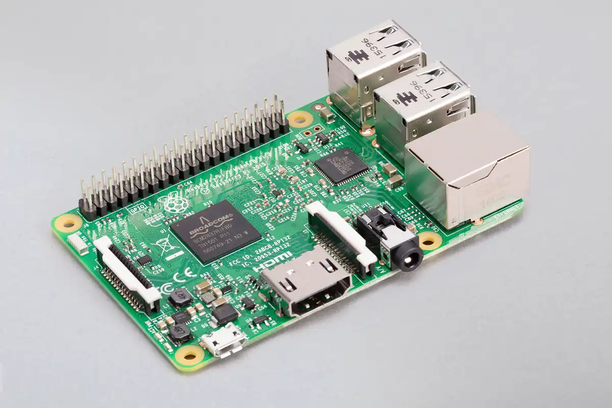
|
|
References:
- Raspberry Pi 3 Model B
- Searched by
Raspberry pi 3Bin DDG
- Searched by
-
Python驱动树莓派SPI接口 - 简书 - 月见樽
- Searched by
树莓派 SPI 实验in DDG
- Searched by
Notes:
- Use the python library
spidevto drive the SPI interface. (r2-简书)
UART
References:
(2024-10-13)
-
UART那么好用,为什么单片机还需要I2C和SPI? - bilibili - 工科男孙老师
- Searched by
I2cin Bilibili
- Searched by
- Universal asynchronous receiver-transmitter - Wikipedia
-
Windows下通过串口连接树莓派 Raspberry Pi (USB to TTL, PuTTY) - bilibili - 老刘玩机
- Searched by
树莓派3D 串口 实验in bilibili
- Searched by
-
KingstVIS 逻辑分析仪使用介绍 - 伊红美兰 - 博客园
- Searched by
逻辑分析仪 用法in DDG
- Searched by
Notes:
(2024-10-23)
-
UART: Univeral Asynchronous Receiver - Transmitter
-
Univeral:
-
Asynchronous:
-
SPI is Synchronous, and it needs an independent clock wire (SCK) to synchronize the bits transmission and receiving (Spi-Bili 03:13, Ardu-Ytb 01:16, Ardu-Doc). Whereas, the UART is Asynchronous, and there is no a clock wire.
-
For I2C bus, it is the SCL wire that synchronizes the clocks of the two participants to interpret (encode/decode) the signal (instruction/data) with correct timing. Arduino Docs
-
-
Baud rate:
::: aside
- References: {{{
-
A demo of the I2C communication between Arduino and MPU6050.
How I2C Communication Works and How To Use It with Arduino - YouTube - How To Mechatronics- Directed by I2C总线和通信协议详解 (超详细配42张高清图+万字长文) - 知乎(2024-10-13)
- Searched by
I2C 可以与哪些设备通信in DDG - Blog and code: How I2C Communication Works? Arduino and I2C Tutorial by Dejan
-
A demo of the I2C communication between Arduino and MPU6050.
-
Three Drawbacks and Enhancements (r1-Bili)
-
UART cannot transmit data via a long distance due to the TTL voltage, which is easily interfered.
Variant:
-
RS-232
(2024-11-29)
- Uses 4 wires: TX, RX, GND, VCC r3-bilibili
-
RS-485 supports 1 km transmission.
-
-
Speed is limited by the baud rate, which depends on the conformity of their own clocks. However, the clock is not precise enough to guanrantee the agreed buad rate.
Variant:
- SPI uses a shared clock wire to determine when to fetch a bit from the SDA line.
-
UART communication is confined to only two devices.
Variant:
- I2C applies a bus to allow communication between any two devices mounted on the bus.
Sending data byte-by-byte:
- Start bit r2-Wiki

(2024-12-13)
- Waveform on logic analyzer r4-博客园
Serial
References:
-
Serial communication - Wikipedia
- Searched by
Serial communication protocolin [DDG](Serial communication protocol)
- Searched by
Notes:
